Lab 7
The Advanced Encryption Standard
The goal for Lab 7 was to perform 128-bit AES (Advanced Encryption Standard) encryption on hardware to send a plaintext message and key from the MCU to the FPGA accelerator and recieve back correct cyphertext.
The MCU code was provided to send a key and plaintext message over SPI to the FPGA and check that the result is correct, so there was no coding in C that needed to be done for this lab. We were concerned with the AES implementation on the FPGA, which included developing our FSM and the many submodules needed for complete encryption. The block diagram for my FPGA code is included below.
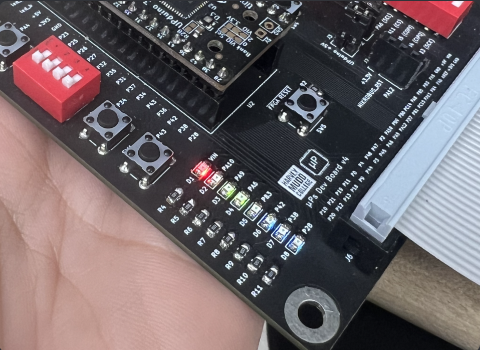
For this lab, I met both proficiency (which invovled getting testbenches to pass in simulation) and excellence (which involved getting FPGA code to actually fit on hardware). I was able to meet excellence specs, as seen in the image below which shows the LED A9 on to indicate a correct cyphertext output.
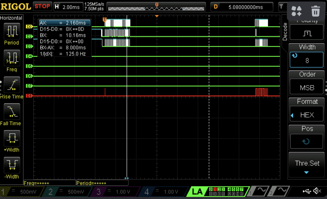
This means that we would be able to visualize the SPI transactions occuring between the MCU and the FPGA on the logic analyzer. The image below shows the entire 128-bit transaction: the first chunk of signals includes the transmission of the key and plaintext, while the second chunk of signals includes the transmission of the cyphertext.
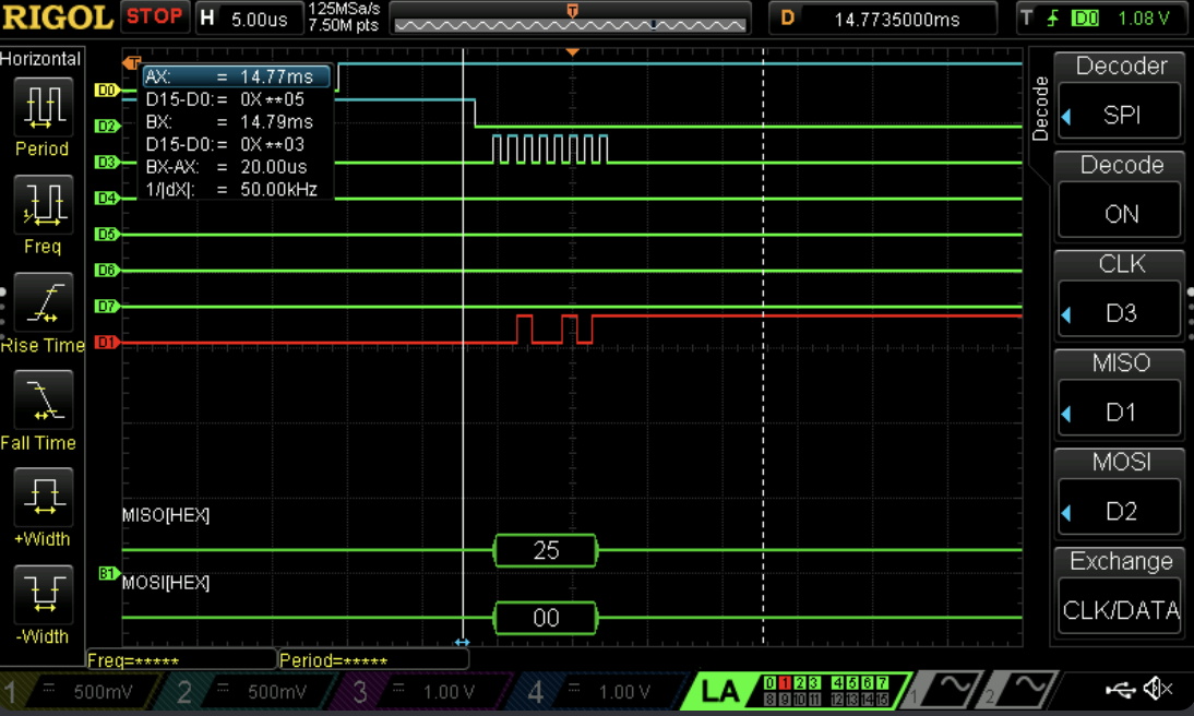
The following images show the specific transactions of the first two bytes of the cyphertext being transmitted accurately. The first byte of the cyphertext is 39 as detailed on page 35 of the AES spec sheet, which is correctly reflected on the logic analyzer shown below.

The second byte of the cyphertext is 25, and we can see this also ouputted correctly on the logic analyzer below.
The debugging process for this lab felt familiar in the beginning when implementing in simulation, but less so once moving into hardware. I felt that the use of waveforms and testbenches was a return to comfortable debugging, which was much welcomed. However, debugging the hardware felt oftentimes pointless because there were less familiar tools to use especially when trying to spot if the issue was with my FPGA code or somewhere else. Ultimately, I used a mix of the Segger debugger tools and investigating Lattice’s cryptic warning messages to try out different things to get it to work in hardware. The final stages of debugging to reach excellency were ultimately long and painful because of my unfamiliarity with FGPA-MCU interactions, but it was rewarding to finally get the lab to work.
This lab took me 24 hours to complete.