Lab 3
Keypad Scanner
For Lab 3, we used an FPGA to scan inputs from a keypad and display outputs sequentially on a double 7-segment dispplay. There were lots of little caveats to the design that accounted for weird button pressing on the part of the user. A key part of this lab was that each key should only register once, regardless for how long it was pressed and if another button was pressed at the same time. These two things affected the way I designed my lab greatly, because we had to account for many different situations in a clever way.
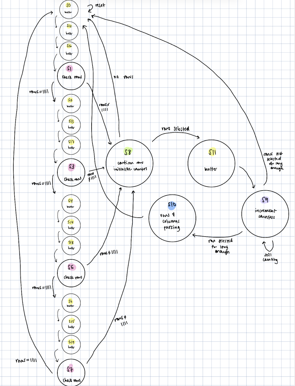
This lab took a lot of pre-thinking and planning in order to fully understand the complexities of what we were tasked to do. In order to start the lab, I started by making an Finite State Machine to understand the flow of the design and what would occur in each state of the design. The State trainsition table followed after.
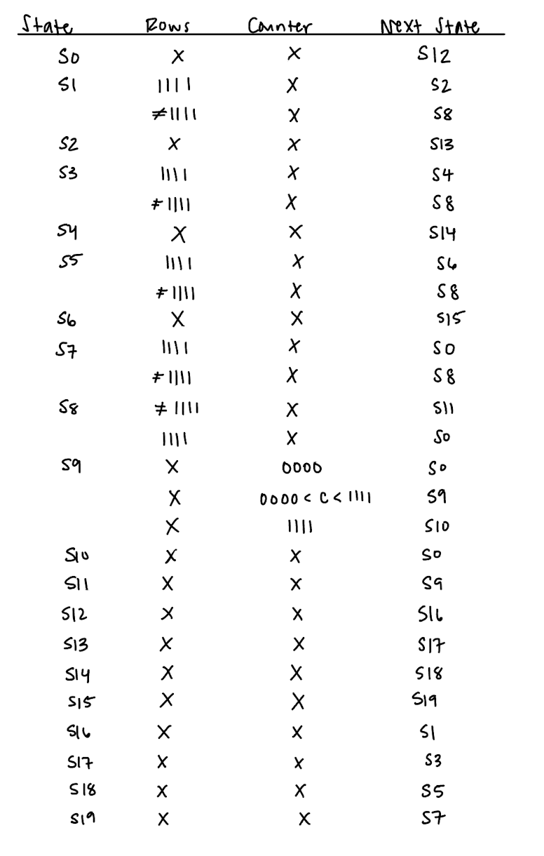
To handle switch debouncing, I initialized counters in State 8 that would increment depending on if the button was pressed/unpressed on the clock cycle. If the counterOn fills up first, then the design will transition forward to actually displaying digits, however, if counterOn fills up first, the the deisgn will reset back to State 0 beacuse the design notices that a button is no longer pressed. This was the most logical way I could think of to ensure that debouncing would not throw off the entire design, and works because it allows for this to be contained in one state. I chose to implement it in the software rather than doing hardware switch debouncing (with a RC-circuit) because I thought that the discharging of the capacitor as a debouncing counter would not be as reliable.
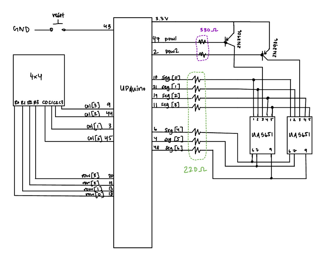
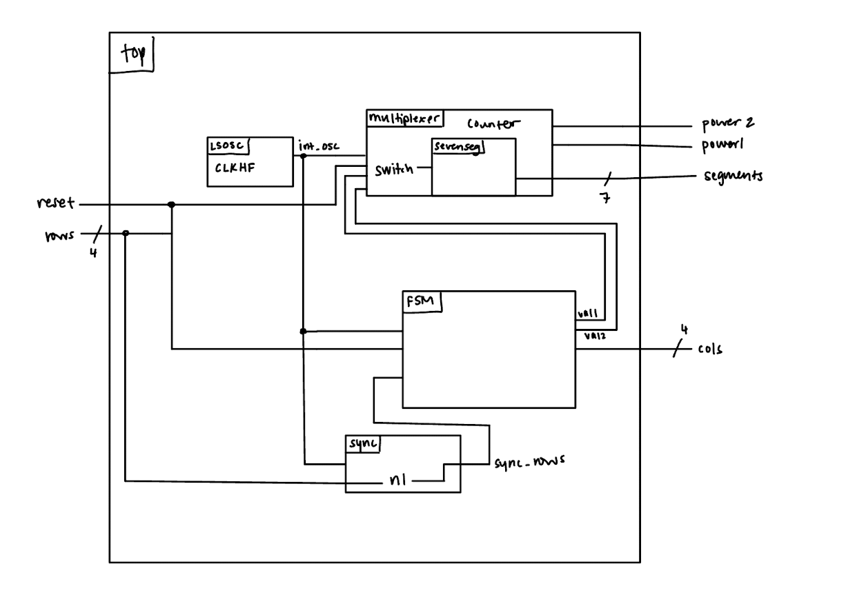
Final schematics and block diagrams of the Verilog are shown below.
I am glad that I started off finalizing the Verilog through simulation before starting the hardware portion. Simulation screenshots are included below.
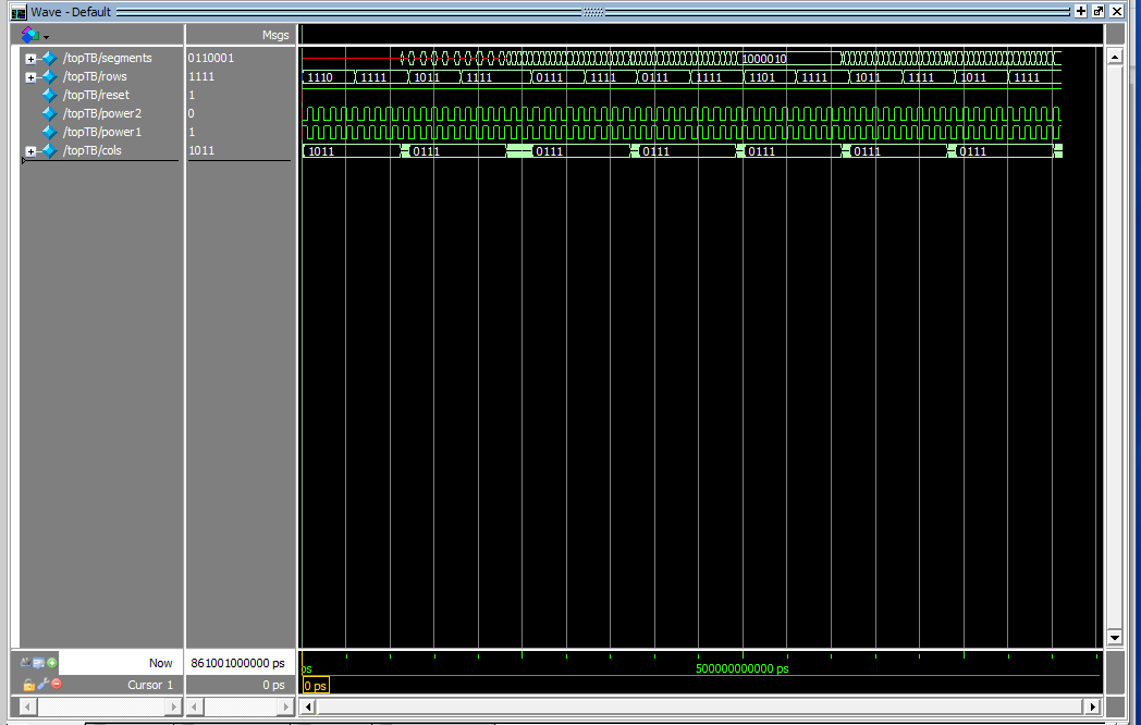
I did not even touch the hardware until the simulation was completely working and this allowed for relatively smooth building of the hardware. I did not really have many problems wiring up the hardware and getting it to work similar to the simulation which was mostly due to the thorough work I did leading up to hardware implementation.
However, debugging towards the final stages was where I ran into a lot of problems. I spoke about it in my reflection for this week, but I had a small bug where pressing other buttons in the same row triggered a display of the first button. I spent a great amount of time addressing this bug. Knowing that it would be a minor fix, I still struggled to find exactly where in my Verilog the edit needed to be made. I did not spend enough time really thinking about WHY the problem was occurring and jumped straight into debugging because I felt like I was so close to being done with the lab. I think skipping over the understanding step ultimately meant I spent way more time on debugging than needed.
Ultimately, I learned a lot from this lab both about handling very complex projects and also about my debugging style.
I spent about 20 hours on this lab