Lab 2
Multiplexed 7-Segment Display
The goals of this lab were to set up a two seven segment display, however, the catch was that we used time multiplexing to efficiently use the I/O on the FPGA. So, using one set of I/O FPGA pins and two transistors, the time multiplexing setup essentially allowed for power to be toggled back and forth on the two displays at a speed too fast to be processed by the human eye, thus appearing as two constant displays instead. In addition to the displays, a set of 5 LEDs also shows the sum of the two numbers being displayed. Schematics and a block diagram are shown below.
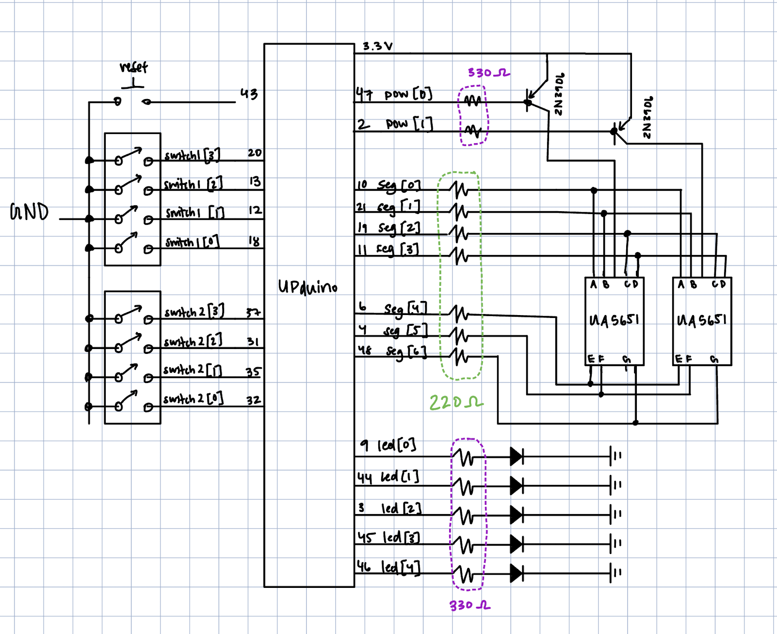
To design the 7-bit display, I first looked at the datasheets to get acquainted with the 7-bit display we were provided with, as we shifted on to a double digit version which was different than the one being used last week. I needed to get acquainted with the hardware pieces first to fully think through the system at hand. I found that thinking through schematics and block diagrams to really visualize the hardware and signal flow was an important first step for a more complex lab like this one.
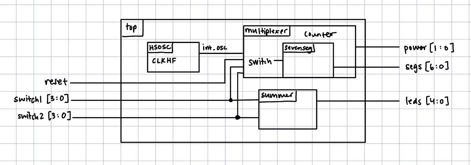
The coding was more complex than last week, and required a thorough note-taking and scribbling thinking process to fully understand the set of inputs, outputs, and dependencies for the entire system. A block diagram is shown below.
There was a long debugging process throughout the entire lab work. First, there were plenty of syntax errors with my SystemVerilog that had to be addressed in order to even flash anything onto the FPGA. Most of this process had to do with addressing compile issues in Lattice Radiant itself. Then, even when code would flash, there were plenty of wiring issues to make sure the switches were arranged in a user-friendly way and that the correct segments were lighting up when needed. The debugging process for the segments of just pulling wires here and there did not work well this time, and it took some further datasheet inspection and fiddling to get this working correctly.
The design meets all requirements. The two digit 7-segment display light up according to bit switch inputs, and the LEDs on the side of the board also light up corresponding to sums.
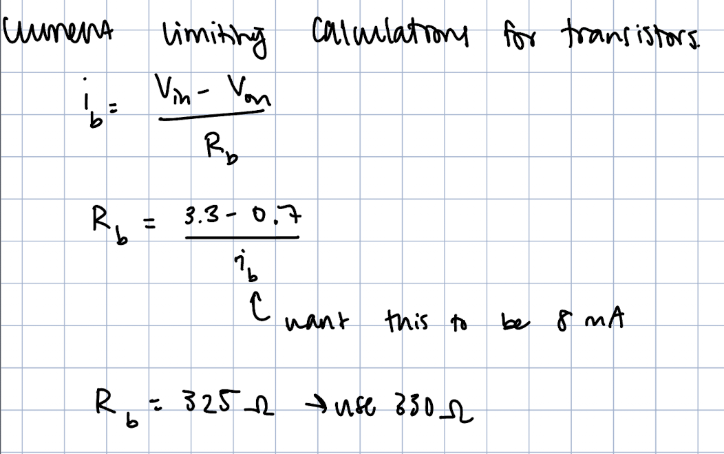
As part of an excellence requirement, I inspected the datasheet further to find desired currents for the FPGA pins, then performed current limiting calculations to find a resistor value that would fit operating conditions.
Current draw/sink on all FPGA pins are below the currents specified in the recommended operating conditions. Claims are backed up by calculations and reference to the appropriate items on the datasheet.
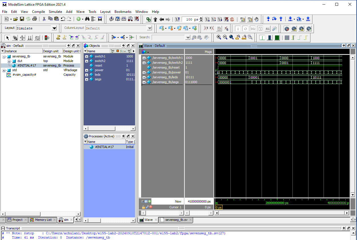
Lastly, I wrote a testbench to simulate that the two digit 7 segment display was working correctly for excellence requirements.
I spent about 12 hours working on this lab.